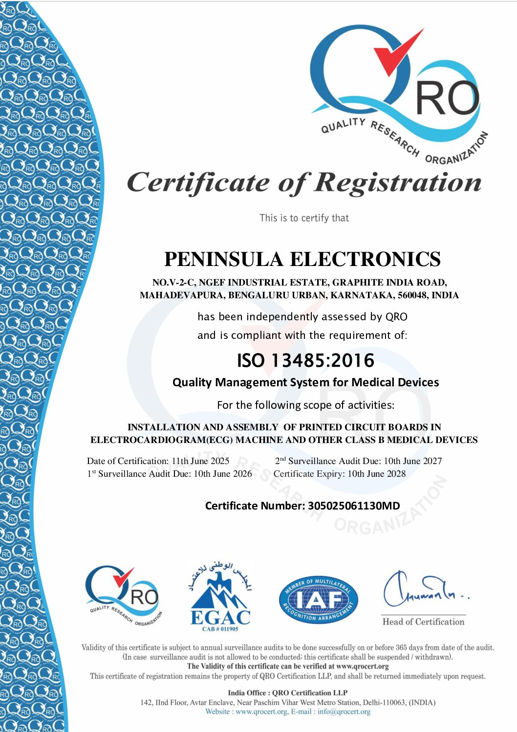
The Resilience of Experience: Navigating India’s EMS Takeoff
The Indian electronics industry has seen a paradigm shift since the establishment of Peninsula Electronics in 1993. What has now become an established pillar of the electronics supply chain began as a nascent industry. Today, India has emerged as the preferred alternate destination for electronic contract manufacturing.
As an industry leader who has seen the electronics industry change over the last three decades, I have come to realize the true value of an EMS provider is not the equipment they have, but the experience they have gained through the years.
Precision Beyond the Board
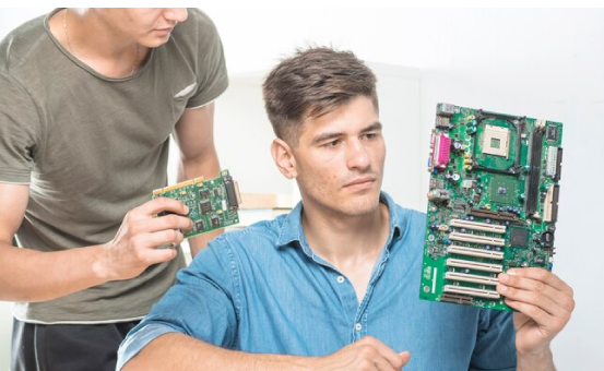
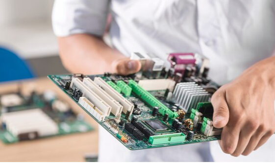
In the current electronic contract manufacturing industry, the scope of board assembly services has far exceeded the basic placement of electronic components. The development of high-complexity industries, such as the aerospace and medical device industries, has brought about a level of technical sophistication that can only come with the refinement of operations over the last few decades. Peninsula has seen these transitions and has refined its SMT manufacturing services to meet the exacting standards of the global electronics industry.
The Integrated Solution: From Prototyping to Box Build
We are currently experiencing an important trend in the electronics industry. OEMs (Original Equipment Manufacturers) are consolidating their supply chain. The new demand is for an integrated solution. This means:
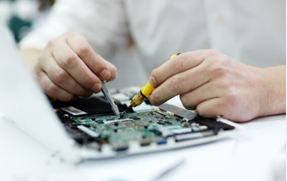
- Advanced PCB Assembly: High density PCBs, flex/regid-flex PCBs with or without Conformal Coating
- Comprehensive Box Build Assembly Services: From Products to Finished Goods Ready for Market Launch
- Local Expertise with Global Reach: As a leading EMS company in India, we are uniquely positioned to assist our partners in capitalizing on the “Make in India” initiative without compromising quality standards.
Why Legacy Matters in a Modern Market
Unlike many others who are entering the EMS Bangalore market to take advantage of the recent growth spurs within the industry, Peninsula Electronics remains committed to the same values that we established our company on in 1993.
Whether it is handling the intricacies of complex PCB assembly of boards for high tech R&D in Bangalore or implementing production strategies for a worldwide rollout, our three decades of experience within the industry guarantee that we don’t just react to the changes within our market – we anticipate them.
Looking Forward
The future of ems electronics will be marked by our ability to quickly respond to industry needs by integrating new technology and environmentally conscious production strategies into our facility.
While our mission remains the same – to be the most reliable link in your electronics value chain – I would like to invite you to get in touch with us to discuss how Peninsula Electronics can bring three decades of excellence to your next project.

Author: Parthasarathy.S
Mr. Parthasarathy is the General Manager at Peninsula Electronics. He brings extensive experience in the electronics industry.


 Ambiguous
 Controlled
 Risky BOM Entry (Ambiguous)